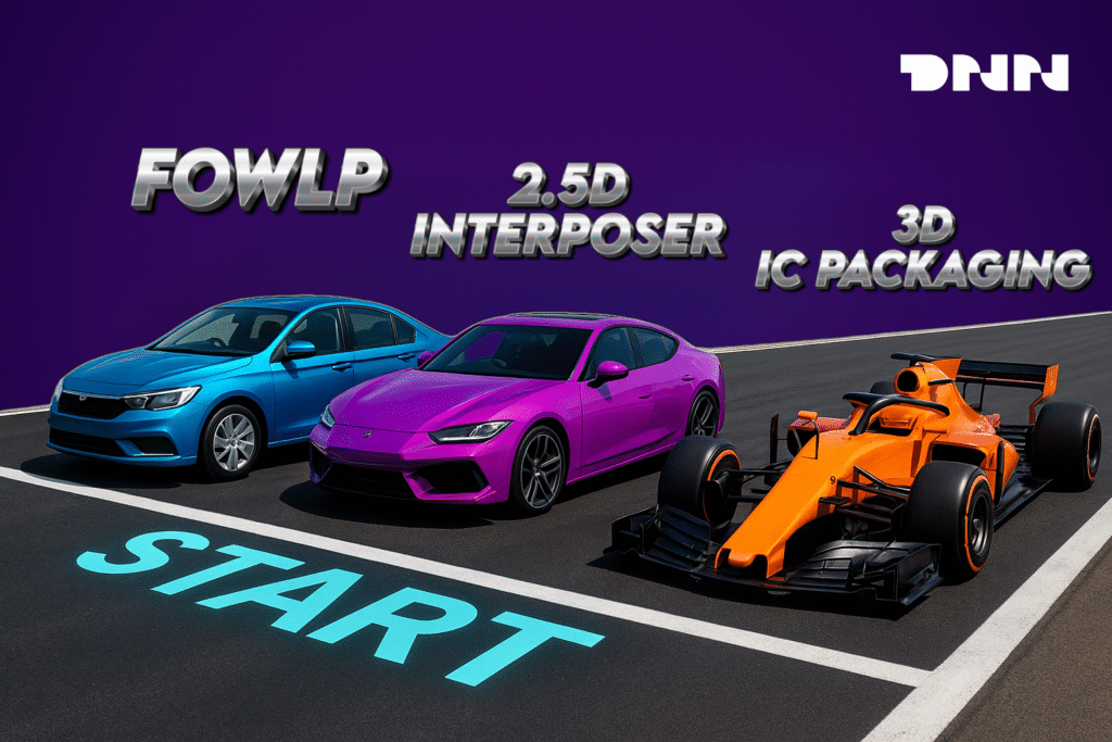
Advanced Packaging Guide (Pt. 5): 2026 Supply Chain, CPO & KGD Market Definition
Recap The first four parts of this guide series have mapped out the evolutionary blueprint of the semiconductor industry in the post-Moore’s Law era. We began in Part 1 by exploring why advanced packaging has become the new frontier of innovation against the backdrop of Moore’s Law’s mounting physical and economic limits ; in Part 2, we delved into how core architectures like 2.5D, 3D-IC, and Fan-Out Wafer-Level Packaging (FOWLP) enable integration solutions that transcend traditional methods ; Part 3 focused on what the Chiplet revolution and the design philosophy of heterogeneous integration entail, explaining the paradigm shift from monolithic Systems-on-Chip (SoCs) to modular designs ; and Part 4 dissected the physical laws that govern this domain, examining the thermal management challenges posed by materials science and multi-physics coupling effects. |
Intro
In this final installment, we will elevate our perspective from technical details to a strategic outlook. This article will delve into the business transformations triggered by Chiplets, analyzing the new roles played by foundries, OSATs, and fabless companies in a reshaped supply chain.
Next, we will look ahead to the future trends defining the next generation of System-in-Package (SiP), including key technologies like Co-Packaged Optics (CPO) and wafer-scale integration. Finally, we will scrutinize the persistent fundamental challenges—from ensuring Known-Good-Die (KGD) to overcoming the physical limits of thermal management—all of which are critical to realizing the full potential of heterogeneous integration.
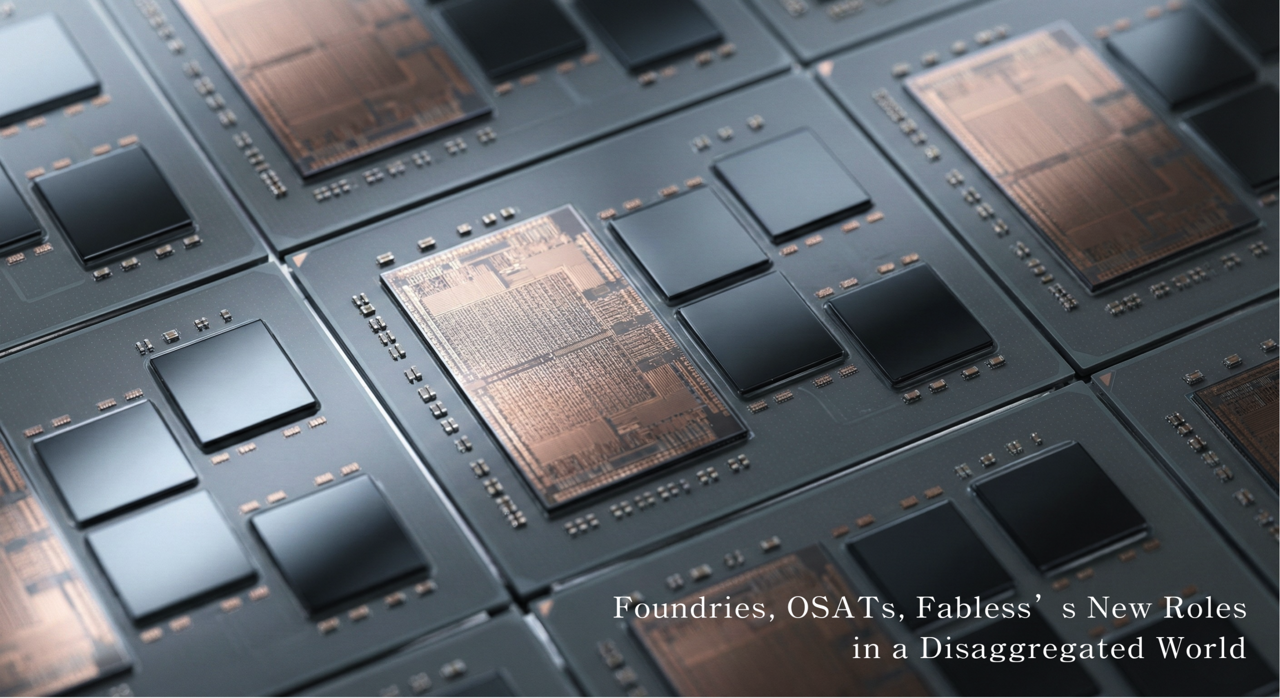
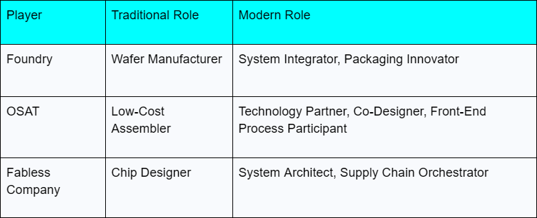
5.1 Foundries, OSATs, Fabless’s New Roles in a Disaggregated World
The central paradox of the chiplet era is that the technical “disaggregation” of the monolithic chip is forcing a strategic and operational “re-integration” of the semiconductor supply chain with unprecedented force. The traditional linear model—where a design house hands off a design to a foundry, which is then passed to an Outsourced Semiconductor Assembly and Test (OSAT) provider—is now obsolete. It has been replaced by a highly collaborative and complex network where the choice of packaging technology is no longer a final step in the back-end process but a core architectural decision that must be made at the very beginning of the design phase.
5.1.1 Foundries: The Rise of the System Integrator
Leading foundries are no longer content to simply manufacture wafers; they are transforming into providers of system-level solutions through vertical integration. They view advanced packaging as a key differentiator to attract and retain high-value customers, especially in the AI/HPC space.
- TSMC’s CoWoS Dominance:
To meet the immense demand from customers like NVIDIA and AMD, TSMC is aggressively expanding its Chip-on-Wafer-on-Substrate (CoWoS) capacity. Projections show its monthly capacity soaring from approximately 35,000 wafers in 2024 to between 70,000 and 90,000 by the end of 2025, with a potential to reach 130,000 by 2026.
This expansion includes new and expanded facilities in Tainan (AP8), Zhunan (AP6B), Chiayi, and Taichung (AP5B). This strategy creates a highly sticky ecosystem where customer dependence on advanced packaging capacity is now as critical as their need for the latest process nodes.
- Intel’s “Systems Foundry” Strategy
Intel considers its Foveros (3D) and EMIB (2.5D) technologies to be the cornerstones of its IDM 2.0 strategy. Its massive $3.5 billion investment in its New Mexico facility is dedicated to advancing Foveros 3D packaging technology. Intel’s portfolio, which includes Foveros-S (silicon interposer), Foveros-R (RDL fan-out), and Foveros-B (silicon bridge), as well as the hybrid EMIB 3.5D architecture, positions the company to transition from a mere chip manufacturer to a provider of “Systems of Chips”.
- Samsung’s Diversified Portfolio:
Samsung is challenging TSMC’s lead with its diverse “Cube” portfolio, including I-CubeS (full silicon interposer), I-CubeE (embedded silicon bridge), and the more cost-effective I-CubeR (all-organic RDL interposer). This tiered product strategy allows Samsung to offer optimal cost-performance solutions for different market segments, from top-tier AI accelerators to cost-sensitive edge computing devices.
At the same time, Samsung is also making substantial investments, including a planned $7 billion for an advanced packaging plant in the U.S. and an R&D center in Japan, aiming to create a complete “one-stop” service from design to manufacturing and packaging.

5.1.2 OSATs: Ascending to Technology Partners
OSAT providers, traditionally seen as low-cost assemblers, are now moving up the value chain to become indispensable technology partners and key players in innovation.
- Deepening Collaboration of ASE and Amkor:
To compete with the integrated solutions offered by foundries, OSATs are actively developing their own advanced packaging platforms (like ASE’s FOCoS) and engaging in unprecedentedly deep collaborations. The most significant trend is TSMC’s decision, driven by the surge in AI chip demand, to outsource its front-end Chip-on-Wafer (CoW) process to ASE’s subsidiary, Siliconware Precision Industries (SPIL), for the first time.
This move represents a major endorsement of ASE’s technical capabilities, as the CoW process is more complex and profitable than the back-end Wafer-on-Substrate (WoS) process traditionally handled by OSATs.
- Building a U.S. Domestic Ecosystem (Amkor and TSMC in Arizona):
The collaboration between Amkor and TSMC in Arizona is a milestone in establishing a resilient, end-to-end domestic supply chain in the U.S. Amkor is investing $7 billion in a large campus in Peoria, Arizona, to provide turnkey advanced packaging and test services—including TSMC’s InFO and CoWoS technologies—for wafers produced at TSMC’s nearby Phoenix fab. This geographic proximity is designed to shorten product cycle times and provide localized supply chain support for key customers like Apple and NVIDIA.
5.1.3 Fabless: The Architects of Systems
Fabless companies are no longer just chip designers; they are now the architects of entire multi-chip systems and have become the primary force driving packaging innovation.
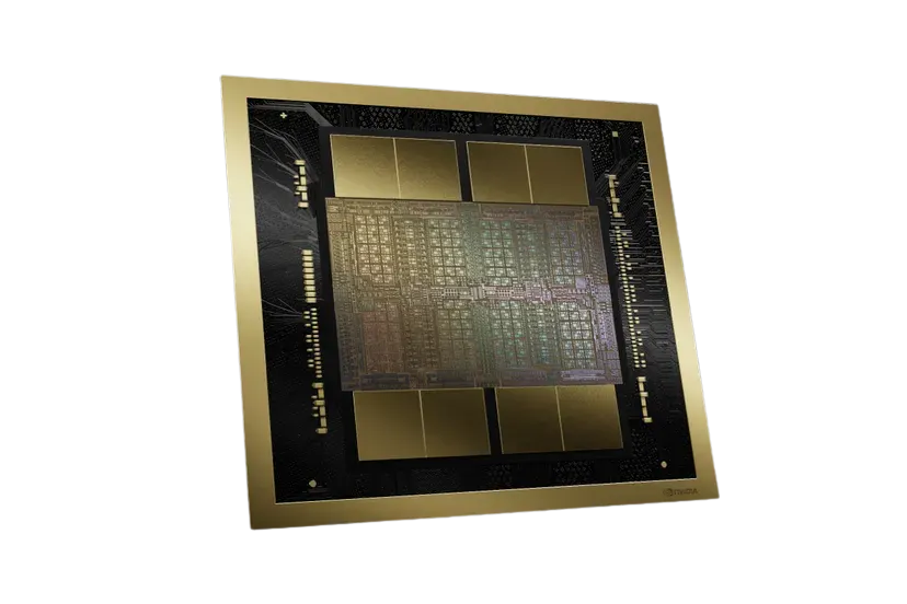
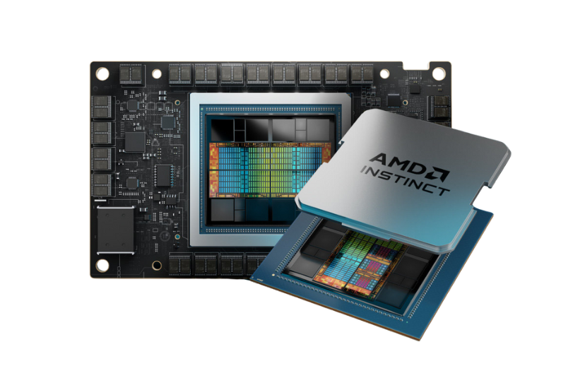
- NVIDIA’s Blackwell Architecture:
The B200 GPU is a prime example of this trend. It features a dual-chiplet design integrated into a single package. These chiplets are connected by a custom 10 TB/s high-speed interconnect, allowing them to function as a single, cache-coherent GPU. This complex design, based on TSMC’s 4N process and CoWoS packaging technology, directly defines the technical requirements for the entire manufacturing chain.
- AMD’s MI300 Series:
The MI300 series showcases a hybrid 2.5D/3D architecture. Its GPU and CPU chiplets (XCDs and CCDs, respectively) are manufactured on TSMC’s N5 process and are 3D-stacked on top of I/O dies (IODs) made with a 6nm process. This complete 3D stack is then placed on a 2.5D silicon interposer alongside HBM3 memory stacks. This advanced “3.5D” approach exemplifies the extreme system-level optimization pursued by today’s fabless design companies.
5.1.4 Re-integration
The fundamental premise of chiplets is the disaggregation of a large, monolithic SoC into multiple smaller, more specialized dies. This seems to point toward a more modular, interchangeable future. However, the performance of the final System-in-Package (SiP) is critically dependent on the physical interconnects between these chiplets.
The choice of packaging technology (e.g., CoWoS or EMIB) and its physical characteristics (e.g., bump pitch, RDL line/space) directly influence and constrain the I/O design of the chiplets themselves.
This interdependence means that chiplets and packages cannot be designed in isolation. A fabless company like NVIDIA cannot simply design a GPU die and “throw it over the wall” to TSMC. The design of the GPU chiplet and the architecture of the CoWoS package must be co-designed and co-optimized through deep collaboration from the very beginning of the project.
This need for co-design shatters the traditional rigid boundaries between fabless design, foundry manufacturing, and OSAT assembly. Today, foundries are deeply involved in package design and assembly; OSATs are being brought into front-end processes; and fabless companies, in turn, are driving the technology roadmap for packaging. Thus, the act of “disaggregating” the chip has paradoxically forced all players in the supply chain to “re-integrate” their operations, strategies, and design flows more tightly than ever before. This is the dawn of the “Great Re-integration.”
5.2 Post-Scaling Technologies: CPO & Wafer-Scale Integration
This section will explore the next wave of packaging innovation that extends beyond the current 2.5D and 3D paradigms. These technologies are aimed at solving future bottlenecks, particularly those related to the limits of electrical signal transmission, chip size, and design complexity.
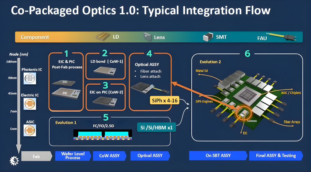
5.2.1 Co-Packaged Optics (CPO): Breaking the Electrical I/O Bottleneck
As the data transfer rates in AI clusters and data centers grow exponentially, the power consumption and limited bandwidth of traditional copper interconnects are increasingly becoming a system-level performance bottleneck.
Co-Packaged Optics (CPO) technology aims to solve this problem by integrating silicon photonics engines directly with electronic Application-Specific Integrated Circuits (ASICs) within the same package. This architecture enables light-based communication, delivering not only a massive leap in bandwidth density but also reducing power consumption by 30% to 50%.
The CPO market is on the cusp of explosive growth, projected to expand from approximately $2 billion in 2025 to over $25 billion by 2033, with a Compound Annual Growth Rate (CAGR) of 40%. Large-scale deployment in data centers is expected between 2028 and 2030. Industry giants such as Broadcom, Cisco, Intel, and NVIDIA have invested heavily in this area, recognizing CPO as a key technology for enabling future high-performance networking and computing.
5.2.2 Wafer-Scale Integration:
Wafer-scale integration represents the most extreme expression of 2.5D integration technology. Instead of dicing a wafer into individual chips, it utilizes the entire 300mm wafer as a single, massive “super-chip,” thereby completely eliminating the boundaries between traditional chips.
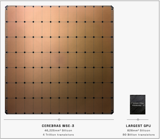
- Case Study: Cerebras WSE-3:
The third-generation Wafer-Scale Engine (WSE-3) from Cerebras Systems is the premier example of this concept. It is a single processing unit built on TSMC’s 5nm process, containing 4 trillion transistors, 900,000 AI-optimized cores, and 44GB of on-chip SRAM.
- Decoupling Compute and Memory:
A key innovation in the Cerebras architecture is the “decoupling” of the on-wafer compute units from external memory. The WSE-3 connects via high-speed interconnects to an external memory system called MemoryX, which can scale up to an astonishing 1,200 TB. This allows a single CS-3 system to store and train AI models with up to 24 trillion parameters—a task that would require a massive cluster of thousands of GPUs to accomplish.
This architecture fundamentally solves the memory capacity limitations inherent in GPU designs, where HBM memory is tightly coupled with the compute die.
5.2.3 AI-Driven Design:
The design space of a multi-chiplet system is astronomically large, making manual optimization of its partitioning, layout, and multi-physics analysis impractical. As a result, the industry is becoming heavily reliant on AI-driven Electronic Design Automation (EDA) tools.
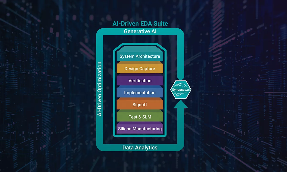
- Synopsys.ai:
Synopsys is a leader in this field. Tools in its Synopsys.ai suite, such as 3DSO.ai and 3DIC Compiler, use AI to automate and optimize the multi-die design flow. A key customer success story demonstrated that 3DIC Compiler reduced the HBM3 routing time on Samsung’s I-CubeS technology from several days to just 4 hours, shortening the overall design cycle by a factor of 10. Furthermore, Synopsys.ai Copilot utilizes generative AI to further accelerate workflows like RTL generation and verification.
- Cadence Cerebrus AI Studio:
Cadence’s platform employs “Agentic AI” to orchestrate the entire SoC implementation flow, allowing a single engineer to manage the design of multiple blocks simultaneously. In a successful collaboration with the Samsung Austin R&D Center (SARC), the platform achieved a 4x overall productivity improvement on an SoC subsystem, along with an 8% to 11% improvement in PPA (Power, Performance, and Area).
5.2.4 Interdependent Solutions
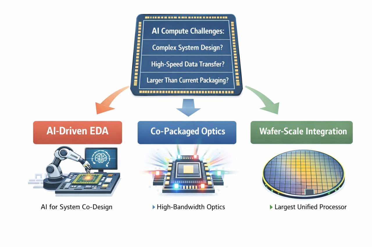
We must recognize that the demand for AI computation is growing at an exponential rate, far outpacing the gains offered by traditional process scaling. This has forced designers to use chiplets to build larger, more complex systems, such as NVIDIA’s Blackwell and AMD’s MI300—an architectural solution.
However, this architectural solution has created three new and significant bottlenecks: (A) How do you design such a complex system? (B) How do you get data into and out of this system fast enough? (C) What if you need a system larger than what current packaging technology can accommodate?
These three “future frontiers” are not independent research paths but a tightly coupled, co-evolving suite of solutions aimed at sustaining the trajectory of AI compute. AI-driven EDA is the direct answer to bottleneck (A), as the system complexity has surpassed human capability, requiring AI to manage multi-physics co-design and layout planning. Co-packaged optics is the direct answer to bottleneck (B), as electrical I/O has hit physical limits of power and bandwidth, necessitating the introduction of photonics to “feed” the computational beast. And wafer-scale integration is the direct answer to bottleneck (C), representing the logical extreme of 2.5D integration to create the largest possible “single” processor and minimize inter-chip communication latency.
In summary, you cannot design a wafer-scale engine without AI-driven tools, nor can you connect multiple such systems into a supercomputer without optical interconnects. They are the three legs of the same stool supporting the future of AI hardware, and none can stand alone.
5.3 Immutable Laws: Persistent Physical and Economic Challenges
This section will delve into the fundamental, recurring challenges that act as the primary constraints on innovation in advanced packaging. These are not problems that can be “solved once” but require a continuous struggle against the laws of physics and economics.
5.3.1 Known-Good-Die (KGD) Testing
The core economic principle of a chiplet system is that a single defective chiplet, costing perhaps a few hundred dollars, can render an entire SiP, worth thousands of dollars, useless. This financial risk grows exponentially with the number of chiplets in a package. If a package contains ‘n’ chiplets, and each has a yield of ‘Y’, the final package yield is approximately Yn. For example, even with a high single-chiplet yield of 95%, the overall yield for a 5-chiplet package drops to 77%; for a 10-chiplet package, it plummets to just 60%.
This makes “Known-Good-Die” (KGD) testing—ensuring every die is fully functional before assembly—the most critical economic challenge. However, the high cost of probe cards and the difficulty of performing at-speed testing at the wafer level make achieving 100% KGD coverage prohibitively expensive.
- Test Standardization:
To address this, the industry is turning to standards like IEEE 1838 (Standard for Test Access Architecture for Three-Dimensional Stacked Integrated Circuits). This standard defines a die-centric test architecture, including features like a Die Wrapper Register (DWR) and “Test Elevators,” to ensure that individual dies and their interconnects can be tested both before and after stacking. This provides a common framework for interoperability and testability in a multi-vendor ecosystem.
5.3.2 KGD as an Economic Manifestation of the Thermal Challenge
The core of the KGD problem is that a single failed die requires scrapping the entire multi-chiplet package. This is an economic problem of yield loss. However, one of the primary reasons a die fails after assembly is thermo-mechanical stress. As the package heats up during operation, the CTE mismatch causes warpage and stress, which over time can lead to the failure of interconnect structures like solder ball cracks.
Thus, a “known-good-die” that passes initial wafer-level tests can fail once it is integrated into a package and subjected to stresses it never experienced in isolation.
This means the KGD problem is not just about finding pre-existing manufacturing defects, but more critically, about being able to predict which dies will become defective under the thermal and mechanical stresses of the final packaged system.
This prediction requires sophisticated multi-physics simulation (the focus of Part 4 of this guide). Designers must simulate the coupled electro-thermo-mechanical feedback loops to identify high-stress points and potential failure modes before manufacturing. In this light, the economic problem of KGD and the physical problem of thermal management are two sides of the same coin.
The financial risk of scrapping a package due to a failed die is the direct economic consequence of our inability to perfectly predict and mitigate the physical effects of thermo-mechanical stress. Therefore, improving KGD yield is inextricably linked to advancing our capabilities in multi-physics co-design and thermal management.
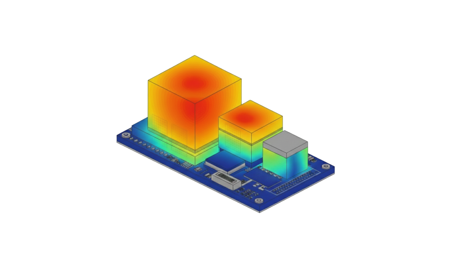
5.3.3 The Thermal Wall: Managing Heat at Extreme Densities
Speaking of thermal management, heat dissipation is the ultimate physical bottleneck in advanced packaging. The power densities in 3D stacks and high-density 2.5D systems are so extreme that removing hundreds of watts of heat from a few square centimeters is a monumental challenge.
- Physics of Failure (CTE Mismatch):
A pervasive reliability challenge stems from the thermo-mechanical stress caused by the mismatch in the Coefficient of Thermal Expansion (CTE) between different materials. A silicon die (CTE ~3 ppm/°C) expands and contracts at a much lower rate than an organic substrate (CTE ~17-50 ppm/°C).
This discrepancy causes the package to warp during temperature cycles, leading to catastrophic failures like solder joint cracking and delamination. This is the fundamental reason why the multi-physics co-design approach emphasized in Part 4 is so essential.
- Advanced Thermal Interface Materials (TIMs):
The industry is moving from traditional thermal pastes to more advanced metal-based thermal interface materials. These include solder TIMs (sTIMs) with high thermal conductivity (approx. 86 W/mK), liquid metals, and compressible TIMs (like Indium Corporation’s Heat-Spring®). These materials are critical for TIM1 (die-to-lid) and TIM1.5 (die-to-heatsink) applications in high-performance AI accelerators.
- The Future of Liquid Cooling (Microfluidics):
For the most extreme thermal challenges, especially in 3D stacks where heat is trapped between layers, traditional air cooling is insufficient. The future lies in direct liquid cooling technology. Pioneering research from companies like Microsoft has demonstrated microfluidic cooling, where microscopic channels are etched directly into the back of the silicon die.
This allows coolant to flow through the chip itself, with a heat removal efficiency up to three times higher than advanced cold plates, enabling greater performance and overclocking potential.
5.3.4 Ecosystem Standardization
Furthermore, as we discussed in the previous chapter, the vision of a truly open, “plug-and-play” chiplet marketplace depends entirely on robust and widely adopted standards.
- The Role of UCIe:
The Universal Chiplet Interconnect Express (UCIe) is the most critical standard, aiming to become the “USB for chiplets”. It defines the complete chip-to-chip communication specifications, from the physical layer and protocol to the software stack.
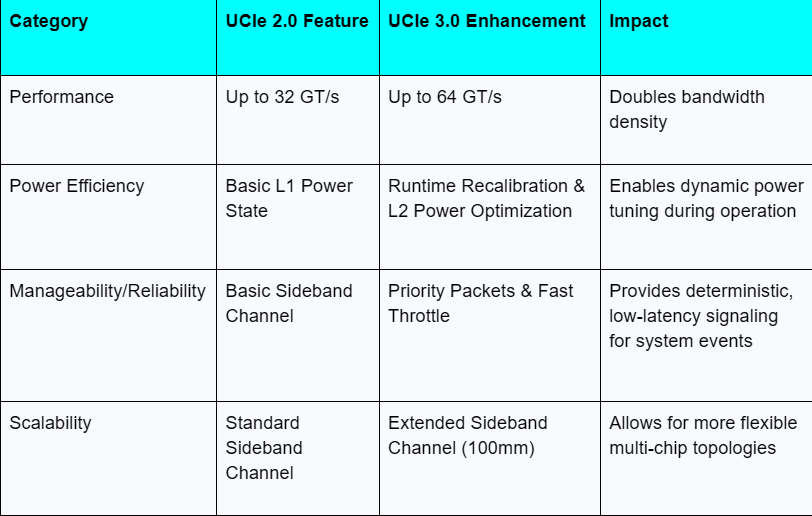
- The UCIe 3.0 Specification:
Released in August 2025, the UCIe 3.0 specification represents a major leap forward. It doubles the maximum data rate to 64 GT/s and enhances power efficiency with features like runtime recalibration and L2 power state optimizations.
It also improves system manageability with an extended sideband channel (up to 100mm), priority packets, and fast throttle/emergency shutdown mechanisms. Crucially, it is fully backward compatible with previous versions.
While UCIe 3.0 is a huge step, building the complete infrastructure for a trusted, multi-vendor ecosystem—including interoperability verification, supply chain security, and clear business models for liability—remains a long-term endeavor that will take years to fully mature.
Conclusion: The Irreversible Shift Toward System-Level Integration
The five parts of this guide series have collectively painted a clear picture: the slowdown of Moore’s Law is not an end but the beginning of a new era—an era of innovation centered on packaging.
From exploring why advanced packaging is necessary, to dissecting its various technological architectures, to analyzing the design philosophy of chiplets and heterogeneous integration, and delving into the underlying physical challenges, we have witnessed a profound industry transformation.
Future computing performance will no longer be determined solely by transistor scaling but by the holistic, co-optimized design of the entire system. The new battlegrounds have shifted to materials science, multi-physics simulation, supply chain integration, and the development of open standards.
Ultimately, the companies and engineers who successfully master the art of system-level integration—those who can precisely balance the complex trade-offs between power, performance, area, and cost (PPAC) at the package level—will define the next generation of technology, from exascale AI computing to ubiquitous intelligent devices.
The era of system-in-package is not coming; it is already here.
about dnn tECHNOLOGY
Headquartered in Taiwan, DNN Technology is a global leader in semiconductor equipment and comprehensive solutions, specializing in used semiconductor equipment trading, laboratory and cleanroom systems construction, and technical consultancy services. With over two decades of industry experience and a team comprising more than thirty experienced technical experts, DNN Technology has successfully executed projects across over fifty countries, committed to providing customized, innovative, and efficient solutions.