Advanced Packaging Guide (Pt. 1): Why 2.5D & Chiplets Are the Mainstream Choice After Moore's Law?

For over half a century, the semiconductor industry’s progress was charted by the predictable cadence of Moore’s Law. Yet, as the physical and economic limits of shrinking transistors come into sharp focus, a new frontier has emerged.
The path to greater performance, power efficiency, and functionality now runs through advanced packaging. This first article in our series explores this fundamental shift, establishing why packaging has become the epicenter of innovation. We will define the core concepts and key terminology you need to know and explain the critical paradigm shift from monolithic Systems-on-Chip (SoCs) to modular, multi-chip Systems-in-Package (SiPs).
1.1 Beyond Moore's Law: Why Packaging is the New Frontier
The predictable, exponential improvement described by Moore’s Law has been the engine of the semiconductor industry for over half a century. Yet, as transistor dimensions shrink to the atomic scale, the challenges of quantum tunneling, heat dissipation, and skyrocketing fabrication costs have become formidable barriers.
Simply making transistors smaller is no longer the most economically or technologically viable path to greater performance. This slowdown in traditional scaling has not, however, diminished the world’s appetite for computational power. On the contrary, the rise of transformative technologies such as Artificial Intelligence (AI), High-Performance Computing (HPC), 5G telecommunications, and autonomous automotive systems has created an unprecedented demand for processing capability, data throughput, and energy efficiency.

To bridge this gap between slowing scaling and accelerating demand, the industry has shifted its innovative focus from the front-end of wafer fabrication to the back-end of packaging. Advanced packaging is a collection of sophisticated manufacturing processes that combine multiple, often dissimilar, semiconductor chips into a single, highly integrated electronic package.
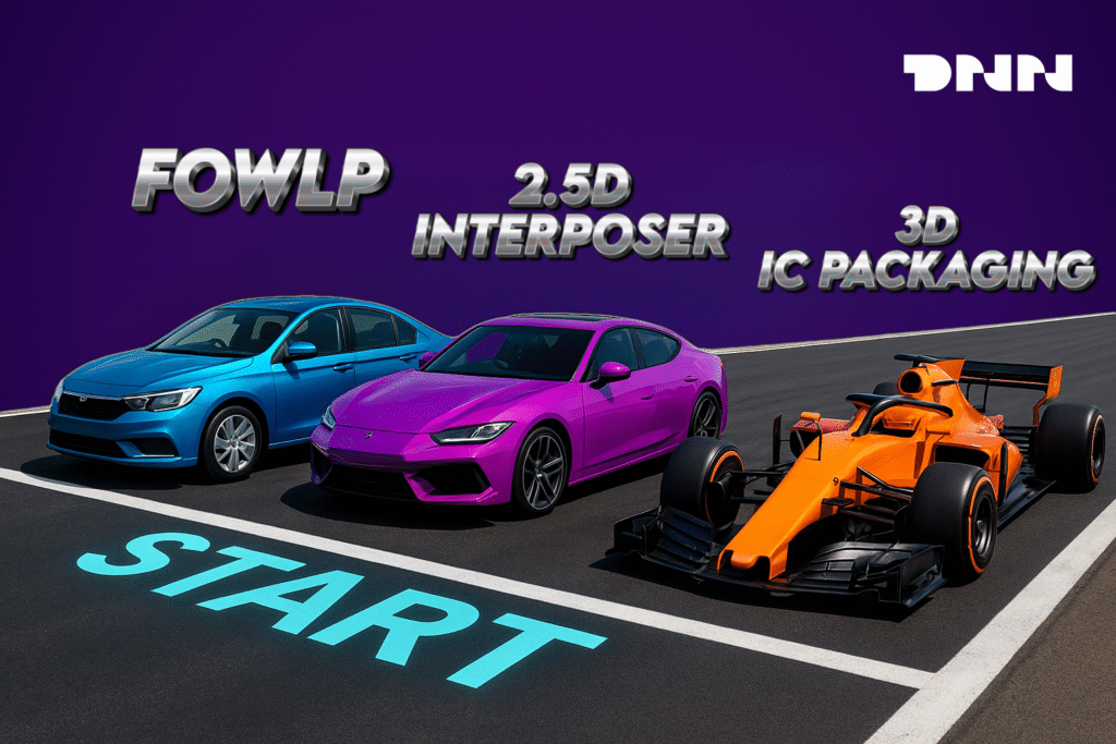
This approach moves beyond the single-chip-per-package model, allowing designers to overcome performance bottlenecks, reduce power consumption, and lower system costs by arranging chips in dense 2D, 2.5D, or 3D configurations.
This strategic pivot has elevated packaging from a protective afterthought to a primary driver of system performance and a key point of differentiation. The objective is no longer just to protect the silicon die but to enable new levels of functionality by optimizing the Power, Performance, Area, and Cost (PPAC) equation at the package level. In this new era, the package itself has become a point of innovation, fundamental to realizing the immense computing capabilities required by the next generation of electronics.

1.2 The Packaging Lexicon: Core Concepts and Terminology
To navigate the complex landscape of advanced packaging, it is essential to first understand its fundamental components. These building blocks, and their evolution, form the basis of all modern packaging architectures.
- Die/Chiplet: At the heart of any package is the die, a rectangular block of semiconductor material cut from a larger wafer. It contains the integrated circuits designed to perform specific functions. The term chiplet has emerged to describe a die that is specifically designed not to function alone, but to be integrated with other chiplets within a multi-die package to form a complete system.

- Substrate: This is the foundational platform, typically a laminate material like FR4 or polyamide, that provides the physical structure and electrical pathways to connect the dies within the package to the external system, such as a Printed Circuit Board (PCB).
- Interconnects: These are the conductive pathways that transfer electrical signals and power. The methods of interconnection have evolved significantly.
- Wire Bond: A traditional and cost-effective method where thin wires connect pads on the top surface of a die to the leadframe or substrate. This method is limited by the length of the wires and the fact that connections can only be made around the periphery of the die.
- Flip-Chip: A more advanced method where the die is “flipped” upside down. Solder balls, or bumps, are deposited on the active face of the die, allowing it to be directly attached to the substrate. This enables connections across the entire surface of the die (an area-array), providing many more I/O points and much shorter, lower-inductance electrical paths compared to wire bonds.

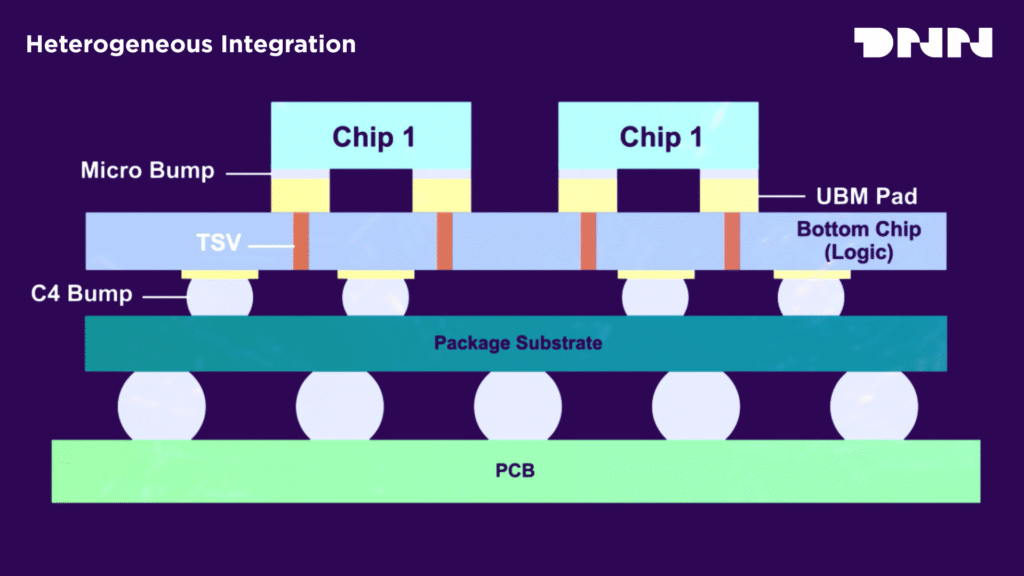
- Interposer: A critical component in 2.5D packaging, an interposer is a high-density intermediate layer that sits between the active dies and the main package substrate. It acts as a sophisticated routing bridge, providing ultra-fine-pitch interconnects that are not possible on a standard organic substrate. Interposers are typically made of silicon, organic materials, or glass.

- Redistribution Layer (RDL): An extra layer of metal traces and dielectric material fabricated on top of a wafer or a molded package structure. Its purpose is to “reroute” the I/O pads from their original locations on the die to a new array of contact points. This is a core technology for both Fan-Out packaging and creating the dense connections on an interposer.
- Through-Silicon Via (TSV): A revolutionary technology that creates a vertical electrical connection passing completely through a silicon wafer or die. By turning the silicon itself into an interconnect, TSVs are the fundamental enabler of 3D die stacking, allowing for the shortest possible communication path between vertically stacked chips.
The history of these components reveals a clear and consistent narrative: a relentless pursuit of shrinking physical distances. The progression from long, peripheral wire bonds to the shorter, area-array connections of flip-chips was the first major leap. The next bottleneck became the horizontal distance between separate chips on a PCB. This was solved by the introduction of the interposer in 2.5D packaging, which uses RDLs to place dies much closer together, drastically shortening the die-to-die communication path.
Finally, 3D-IC technology takes this to its logical conclusion by stacking dies vertically using TSVs, effectively eliminating horizontal distance altogether to achieve the absolute shortest path possible. This entire history of packaging innovation can be understood as a continuous battle against the physical limitations of signal propagation—latency and power loss—by bringing dies ever closer together.
1.3 System-on-Chip (SoC) vs. System-in-Package (SiP): A Paradigm Shift
The evolution of packaging technology has enabled a fundamental shift in design philosophy, moving from a monolithic approach to a modular one. Understanding the distinction between a System-on-Chip (SoC) and a System-in-Package (SiP) is crucial to grasping this change.
- System-on-Chip (SoC): The traditional goal of semiconductor integration, an SoC integrates all the necessary functions for a complete electronic system—such as processing cores, memory, I/O controllers, and analog circuits—onto a single, monolithic piece of silicon.
- System-in-Package (SiP): In contrast, a SiP achieves system-level functionality by integrating multiple discrete components into a single package. These components can include one or more processor dies, memory chips, sensors, and passive components, all interconnected within the package. Any of the advanced packaging architectures—2.5D, 3D, or Fan-Out—can be used to construct a SiP.

The industry is now witnessing what has been described as a “reversal of the SoC trend” in favor of modular, SiP-based architectures built from smaller components known as chiplets. This is not merely a technical preference but a profound strategic and economic decision.
The monolithic SoC approach, while elegant in concept, carries significant risks and inefficiencies. It forces all system functions, from high-speed digital logic to sensitive analog I/O, to be manufactured on the same cutting-edge—and thus most expensive—process node, even if many of those functions do not require such advanced technology. Furthermore, a single, microscopic defect on a large, complex SoC can render the entire chip useless, leading to poor manufacturing yields and dramatically increased costs.
The SiP approach, using chiplets, mitigates these issues. It decouples the various system functions from a single, unforgiving manufacturing process. Designers can select the optimal process node for each individual chiplet—for instance, using a 5nm process for a high-performance CPU core while using a more mature and cost-effective 28nm process for the analog I/O chiplet. This “mix-and-match” capability not only reduces cost but also significantly improves overall manufacturing yield.
Because the individual chiplets are smaller, the probability of a defect occurring on any single one is lower. If a defect does occur, only that small, relatively inexpensive chiplet is discarded, not the entire multi-chip system. This shift from a high-risk monolithic philosophy to a flexible, risk-mitigated modular one is driven by powerful economic incentives and is fundamentally reshaping how complex electronic systems are designed and built.
Let DNN Technology Propel Your Next-Generation Design
Navigating the shift from monolithic SoCs to complex SiP architectures requires deep expertise and a reliable partner. The move to 2.5D and chiplet-based designs involves critical decisions in manufacturing, materials, and system-level integration.
At DNN Technology, we don’t just understand these challenges—we solve them. With extensive experience in AP Active Interposer design and a full suite of turnkey consulting services, our team is ready to help you optimize your Power, Performance, Area, and Cost (PPAC) equation.
Contact our expert team today to discuss how we can accelerate your journey into the new era of semiconductor integration.

about dnn tECHNOLOGY
Headquartered in Taiwan, DNN Technology is a global leader in semiconductor equipment and comprehensive solutions, specializing in used semiconductor equipment trading, laboratory and cleanroom systems construction, and technical consultancy services. With over two decades of industry experience and a team comprising more than thirty experienced technical experts, DNN Technology has successfully executed projects across over fifty countries, committed to providing customized, innovative, and efficient solutions.