Advanced Packaging Guide (Pt. 2): 2.5D vs. 3D-IC vs. FOWLP
In the first part of this series, we established why advanced packaging has become the new frontier for semiconductor innovation. Now, we turn our focus to the how. This article provides a deep dive into the core packaging architectures that are enabling the next generation of electronics.
We will explore the technical specifics of each primary technology, starting with the limits of traditional 2D packaging before moving to the powerful 2.5D interposer-based solutions that dominate high-performance computing today. We will then build upwards into the world of true 3D-IC stacking and also explore Fan-Out Wafer-Level Packaging (FOWLP), a critical alternative path for high-density integration.
2.1 The Foundation: 2D Packaging and its Limits
The most basic and long-standing form of packaging is 2D, or planar, packaging. In this traditional model, a single silicon die is typically attached to a laminate substrate or leadframe and encapsulated in a protective plastic or ceramic casing. The electrical connections from the die to the package’s external leads (which then connect to a PCB) are made using either wire bonds around the die’s periphery or a simple flip-chip configuration.

For decades, this approach was sufficient for the vast majority of electronic devices. However, for today’s high-performance applications, the limitations of 2D packaging have become a significant bottleneck. The primary issue is interconnect length. When multiple chips (e.g., a processor and memory) are packaged separately and placed on a PCB, the physical distance the signals must travel between them is substantial.
These long traces on the PCB introduce significant latency (delay), increase power consumption (to drive the signals over the distance), and limit the overall communication bandwidth between the chips. Furthermore, placing multiple large packages on a PCB results in a large physical footprint, which is unacceptable for space-constrained devices like smartphones and wearables. As the demands for speed, efficiency, and miniaturization have grown, the industry has been forced to look beyond the plane of the PCB for solutions.

Due to the excessively long interconnect distances between chips.
2.2 Bridging the Gap: The Rise of 2.5D Integration
As an evolutionary bridge between traditional 2D and full 3D packaging, 2.5D integration emerged as a powerful and pragmatic solution to the interconnect bottleneck.
The core concept of 2.5D is to bring multiple active dies much closer together than a PCB would allow by mounting them side-by-side on a high-density intermediate substrate known as an interposer.
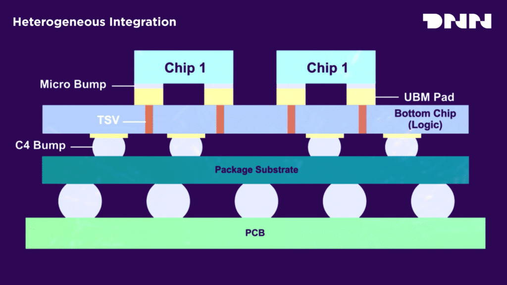
The architecture of a typical 2.5D package is a multi-layered assembly. At the top are the active dies (chiplets), such as a GPU and several High Bandwidth Memory (HBM) stacks. These dies are connected via high-density micro-bumps to the interposer below. The interposer, often made of silicon, contains extremely fine Redistribution Layers (RDLs) that handle the dense, short-distance horizontal routing between the dies.
To connect this entire assembly to the main package substrate, the silicon interposer utilizes Through-Silicon Vias (TSVs) that pass vertically through it, connecting the RDLs on top to a larger grid of bumps on its bottom surface. This entire interposer-and-die assembly is then mounted onto a standard organic package substrate, which provides the final connection to the system’s PCB.


The primary benefit of this architecture is a dramatic reduction in die-to-die interconnect length. By replacing long PCB traces with microscopic RDLs on the interposer, 2.5D packaging significantly improves signal integrity, lowers latency, and reduces the power required for communication.
This makes it an ideal platform for heterogeneous integration, allowing for the close coupling of different types of chips, most notably logic processors with HBM, which is critical for modern AI and HPC systems.
In the landscape of current-generation high-performance systems, 2.5D integration has become the pragmatic workhorse.
While “true” 3D stacking represents the ultimate goal for density and performance, 2.5D offers a mature, high-yield, and thermally manageable solution that directly addresses the most critical bottleneck in AI and HPC: the “memory wall.” This term refers to the disparity between the rapid increase in processor speed and the relatively slow improvement in the speed of data transfer between the processor and main memory.
Placing HBM stacks and a GPU side-by-side on a silicon interposer effectively smashes this wall by creating a massive, ultra-wide, and extremely short communication bus between them.
This architecture is also more thermally manageable than a full 3D stack, where heat from the high-power logic die can become trapped by the memory die stacked on top. In a 2.5D layout, the hot components are adjacent, providing a more direct path for heat to escape upwards to a cooling solution.

Thus, 2.5D is not merely a “lesser” version of 3D; it is the optimal, battle-tested solution for the most pressing problem in high-performance computing today, expertly balancing performance gains with manageable thermal and manufacturing complexity.
2.3 Building Upwards: The Power of 3D-IC Stacking
3D-IC packaging represents the next dimension in semiconductor integration, moving beyond side-by-side arrangements to stack multiple active dies vertically. This architecture creates the shortest possible interconnect paths, unlocking unprecedented levels of performance, power efficiency, and miniaturization.
In a 3D-IC, two or more thinned dies are stacked directly on top of one another. The electrical connections between these layers are forged using vertical interconnects that pass through the silicon itself. In early implementations, these connections were made with micro-bumps, but the leading-edge technology is now direct Copper-to-Copper (Cu-Cu) hybrid bonding.
This advanced technique directly fuses the copper pads on the surfaces of two dies, creating a seamless, high-density connection.
The benefits of 3D stacking are profound and directly address the core goals of modern electronics, often summarized by the acronym SWaP (Size, Weight, and Power). By building vertically, 3D-ICs achieve the smallest possible physical footprint, which is critical for mobile devices, wearables, and aerospace applications.
This density also reduces weight. Most importantly, the extremely short vertical interconnects minimize parasitic capacitance and resistance, leading to superior power efficiency and the highest possible data bandwidth between stacked layers.
The transition from micro-bumps to Cu-Cu hybrid bonding is a foundational technological leap that enables the full potential of 3D integration. Micro-bumps, being tiny solder balls, have a physical limit to how closely they can be spaced (their “pitch“). They also require a polymer “underfill” material to be injected between the dies for structural support, which can impede heat transfer.

Cu-Cu hybrid bonding overcomes both limitations. It allows for much finer interconnect pitches, often below 10 micrometers, dramatically increasing the number of connections possible in a given area and boosting I/O density and bandwidth.
Furthermore, by eliminating the solder and underfill, it creates a more direct and efficient path for heat to conduct between the dies, improving thermal performance. This direct, fine-pitch, metal-to-metal bond is so seamless that it begins to blur the line between a package of discrete chips and a single, monolithic 3D device.
It is this technological shift that is transforming 3D stacking from a niche capability into a mainstream path for future high-performance systems.
2.4 A Comparative Analysis: 2D vs. 2.5D vs. 3D-IC
The choice between 2D, 2.5D, and 3D packaging involves a complex series of trade-offs between performance, cost, and complexity. For system architects and design engineers, understanding these trade-offs is critical for selecting the appropriate technology for a given application. A direct, side-by-side comparison provides a clear and valuable framework for this decision-making process.
The following table distills these complex architectural differences into a scannable format, allowing for a rapid, at-a-glance analysis of their respective strengths and weaknesses.

As the table illustrates, there is no single “best” solution. 3D-IC technology offers the pinnacle of performance and integration density but comes with the highest complexity and cost, particularly regarding thermal management. 2.5D integration provides a balanced approach, delivering significant performance gains over 2D while remaining more manageable than full 3D, making it the current standard for high-end systems like AI accelerators.
Traditional 2D packaging remains the most cost-effective solution for applications where performance and form factor are not the primary constraints. The future of packaging is not one of replacement but of coexistence, with designers choosing the architecture that best fits the specific requirements of their product.
2.5 An Alternative Path: Fan-Out Wafer-Level Packaging (FOWLP)
While 2.5D and 3D architectures represent the high-performance peak of packaging, a distinct and highly important branch has developed in parallel: Fan-Out Wafer-Level Packaging (FOWLP). This technology provides an elegant, cost-effective method for achieving high-density integration, particularly in applications where a costly silicon interposer is not justifiable.
The FOWLP process is fundamentally different from 2.5D. Instead of placing dies onto a pre-made interposer, FOWLP builds the package around the dies. In a typical “chip-first” flow, individual dies are precisely placed face-down on a temporary carrier wafer. An epoxy mold compound is then applied, embedding the dies and creating a new, larger “reconstituted wafer”.
After the carrier is removed, one or more Redistribution Layers (RDLs) are fabricated on top of this molded surface. These RDLs connect to the pads on the die and “fan out” over the surface of the molding compound, creating a new, larger array of I/O contact points where solder balls can be placed.
The primary advantage of FOWLP is its substrate-less design. By eliminating both the traditional laminate substrate and the silicon interposer, it achieves a significantly thinner package profile and lower material cost. This approach offers excellent electrical and thermal performance, making it an ideal choice for high-volume, cost-sensitive, and space-constrained applications, such as the RF transceivers, power management ICs (PMICs), and application processors found in modern smartphones.

To further drive down costs and improve manufacturing efficiency, the industry is advancing from FOWLP to Fan-Out Panel-Level Packaging (FO-PLP). This evolution involves transitioning the manufacturing process from standard round silicon wafers to large, rectangular panels. Panels can accommodate a much larger number of packages simultaneously, maximizing the use of the processing area and significantly reducing manufacturing waste and cost per unit.
FOWLP occupies a unique and vital position in the advanced packaging hierarchy. It provides a clever “middle ground” that delivers a substantial improvement in density and performance over traditional 2D packaging but avoids the high cost and complexity of the silicon interposers used in high-end 2.5D systems.
It is, in effect, the technology that democratizes high-density integration, making advanced packaging accessible for the mass-market consumer electronics that define our daily lives.
2.6 Summary
The semiconductor design toolbox has fundamentally expanded. We’ve seen how 2.5D integration conquers the memory wall in AI and HPC, 3D-IC stacking delivers the ultimate in density and efficiency, and FOWLP provides a cost-effective path for high-volume applications. Each is a powerful solution engineered for a specific challenge.
Choosing the right architecture is a critical strategic decision. DNN Technology’s consulting services provide expert guidance to ensure your project is built on the optimal foundation.
Now, with these physical platforms established, we explore the paradigm they enable. In the next part of our guide: the Chiplet Revolution and the art of Heterogeneous Integration.
about dnn tECHNOLOGY
Headquartered in Taiwan, DNN Technology is a global leader in semiconductor equipment and comprehensive solutions, specializing in used semiconductor equipment trading, laboratory and cleanroom systems construction, and technical consultancy services. With over two decades of industry experience and a team comprising more than thirty experienced technical experts, DNN Technology has successfully executed projects across over fifty countries, committed to providing customized, innovative, and efficient solutions.