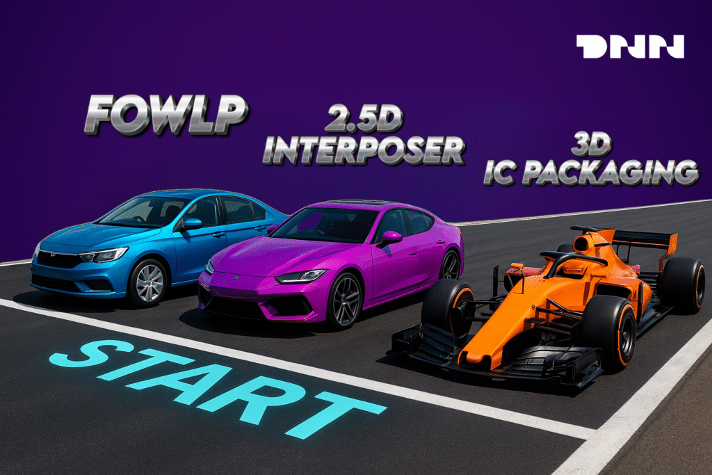
Advanced Packaging Guide (Pt. 3): The Chiplet Revolution and Heterogeneous Integration
The advanced packaging architectures detailed in our previous article are more than just manufacturing techniques; they are the physical enablers of a much larger revolution in system design. This article focuses on that strategic shift. We will explore the move toward disaggregation by defining what “chiplets” are and why they are so compelling.
We will then explain the power of Heterogeneous Integration—the art of mixing and matching these chiplets—and detail the critical role of the Universal Chiplet Interconnect Express (UCIe) standard in creating the open, “plug-and-play” ecosystem of the future.
3.1 The Shift to Disaggregation: What Are Chiplets?
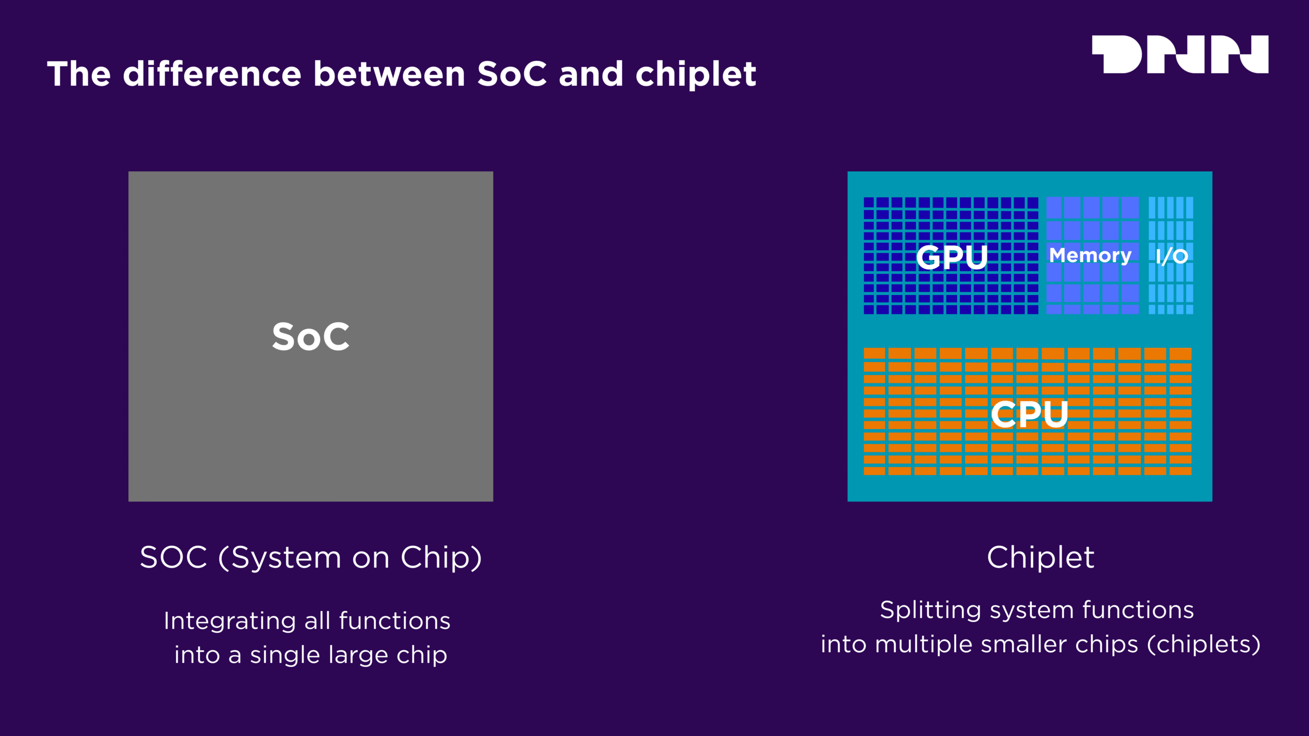
At its core, the chiplet concept represents a move away from monolithic design towards disaggregation. A chiplet is best understood not just as a small chip, but as a new design philosophy. It is an unpackaged die, a discrete functional block, that is specifically designed and optimized to be combined and co-packaged with other chiplets to form a larger, more complex system. This approach effectively breaks down a large, monolithic System-on-Chip (SoC) into its constituent parts, such as CPU cores, I/O controllers, and memory interfaces.
The definition of a chiplet is still evolving within the industry, a hallmark of a rapidly advancing field. Some experts argue that a key feature is the presence of a dedicated, standardized die-to-die interface for communication. Others emphasize the co-design aspect, where a collection of dies are designed from the outset to operate together as a single, cohesive system, regardless of the specific interface used.
Regardless of the precise definition, the benefits of this disaggregated approach are clear and compelling:
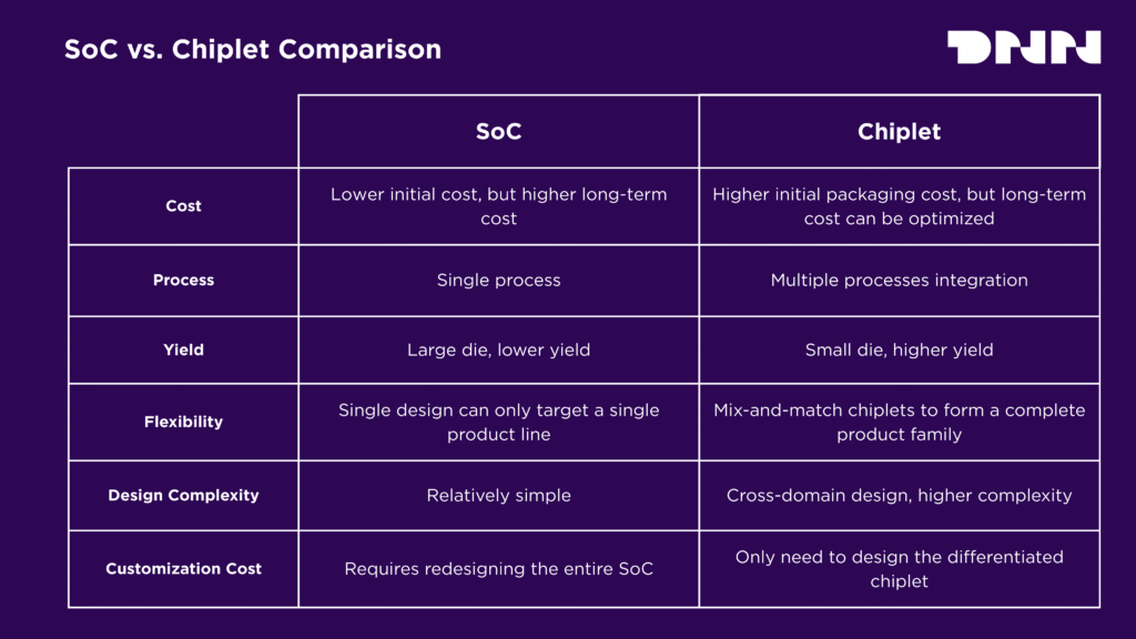
Improved Manufacturing Yield and Lower Cost
Large monolithic chips have a higher probability of containing a manufacturing defect that renders the entire die useless. By breaking the system into smaller chiplets, the yield for each individual component increases dramatically. This allows manufacturers to use only “known-good-die,” significantly reducing overall cost. Furthermore, it allows for the use of the most appropriate and cost-effective process node for each function, rather than forcing everything onto the most expensive leading-edge node.
Faster Time-to-Market and Design Reuse
Once a chiplet is designed and validated, it becomes a reusable block, much like a piece of intellectual property (IP) in a software library. A proven I/O chiplet, for example, can be integrated into multiple product lines with minimal redesign effort, accelerating development cycles and amortizing the initial non-recurring engineering (NRE) costs across many products.
Enhanced Scalability and Flexibility:
Chiplet-based design allows for the creation of entire product families by mixing and matching different chiplets. A company could offer a high-end server processor with eight CPU chiplets and a mainstream version with four, all while using the same I/O and memory chiplets, providing immense flexibility.
The rise of chiplets is creating a new, powerful layer of abstraction in semiconductor design, one that is analogous to the historical shift from transistor-level design to the use of licensable IP blocks in the world of Register-Transfer Level (RTL) design. In the past, creating a custom SoC was a monumental and costly endeavor, accessible only to the largest corporations with vast resources.
Chiplets are the physical manifestation of the IP reuse concept, holding the potential to democratize custom silicon design. In the future, a company could theoretically purchase a CPU chiplet from one vendor, an AI accelerator from another, and a standard I/O chiplet from a third, and integrate them into a unique system tailored to their specific market.
This “plug-and-play” model dramatically lowers the barrier to entry, enabling smaller, more agile companies to focus their resources on designing a single, differentiating chiplet while sourcing the other necessary components “off the shelf”. This paradigm shift is not just about improving yield for large companies; it is a potential catalyst for a new wave of innovation from a much broader range of players, fundamentally changing who can design and build custom chips.
3.2 Heterogeneous Integration: The Art of Mixing and Matching
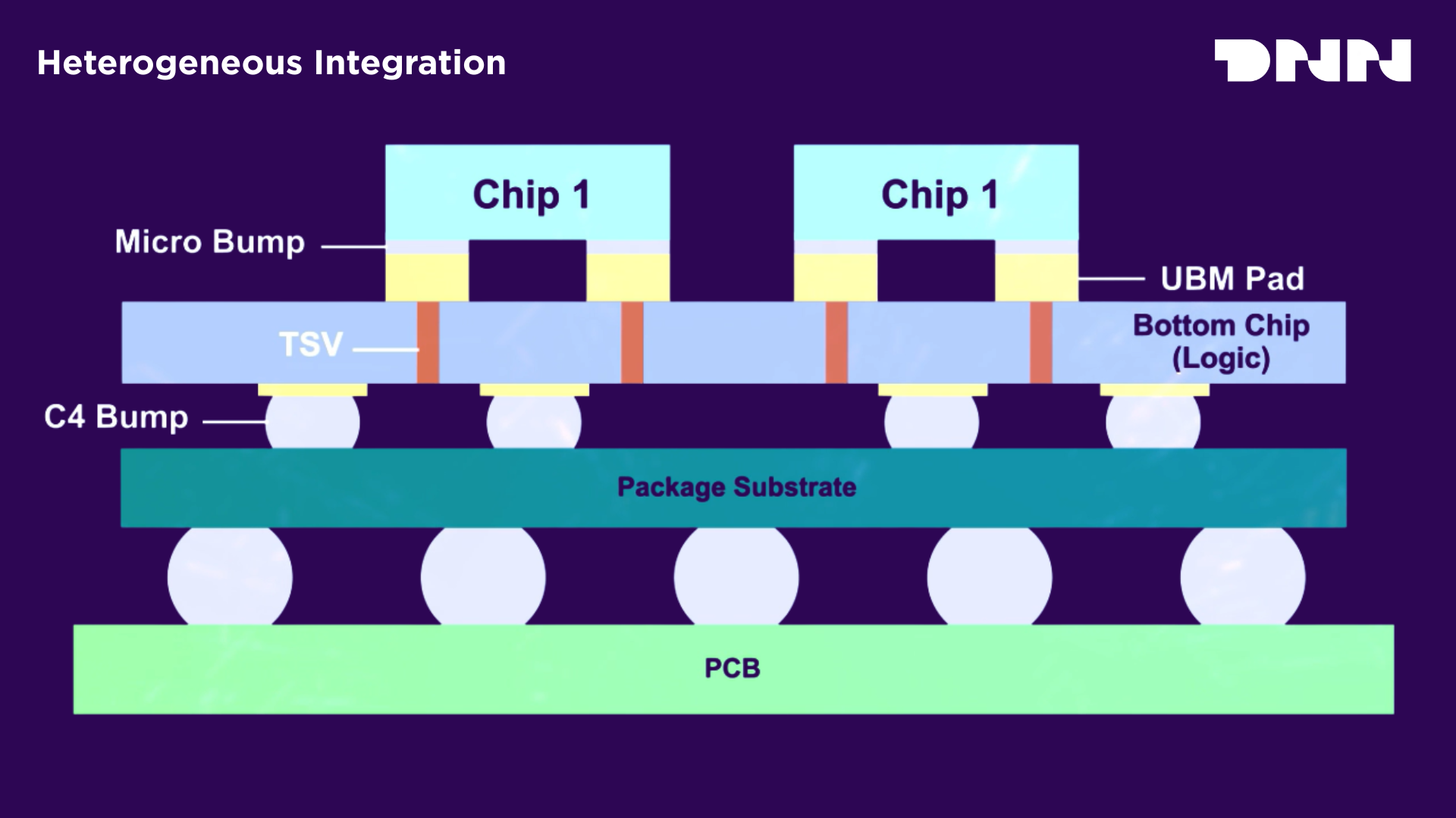
Heterogeneous Integration (HI) is the practical application and ultimate goal of the chiplet design philosophy. It is defined as the assembly of multiple, dissimilar semiconductor components into a single package. These components are “heterogeneous” because they can differ in function (logic, memory, RF, analog), in the process technology they were built on (e.g., 5nm vs. 28nm), and even in the foundry or vendor that produced them.
The advanced packaging architectures discussed previously—2.5D, 3D, and FOWLP—are the physical platforms that make this sophisticated “mix-and-match” approach possible.
Heterogeneous integration marks the definitive end of the “one-size-fits-all” approach that characterized monolithic SoC design. It enables an unprecedented level of optimization at the system level. A monolithic SoC is inherently a design of compromises; the manufacturing process is typically optimized for high-performance digital logic, which is often not ideal for the requirements of sensitive analog circuits, high-voltage power management, or specialized RF components.
HI shatters these compromises. It allows designers to use the absolute best technology for every job. A CPU core can be fabricated on a leading-edge 3nm node for maximum performance and efficiency. The analog I/O chiplets can be built on a mature 28nm node that offers superior signal characteristics and lower cost. High-bandwidth memory can be produced using its own highly specialized DRAM process. Emerging technologies like silicon photonics for optical I/O can be integrated alongside traditional electronics.
The final integrated system is therefore not just the sum of its parts; it is a synergistic whole that can outperform a monolithic equivalent in performance, power, and cost because every single component has been individually optimized on its ideal technology platform. This achieves a level of system-level performance that was previously unattainable.
3.3 Creating a Common Language: The Universal Chiplet Interconnect Express (UCIe)
For the full potential of a chiplet-based, heterogeneously integrated ecosystem to be realized, a critical piece of infrastructure is required: standardization. Without a common, open standard for how chiplets from different vendors communicate with each other, the “plug-and-play” vision remains confined to the proprietary, closed ecosystems of large, vertically integrated companies.
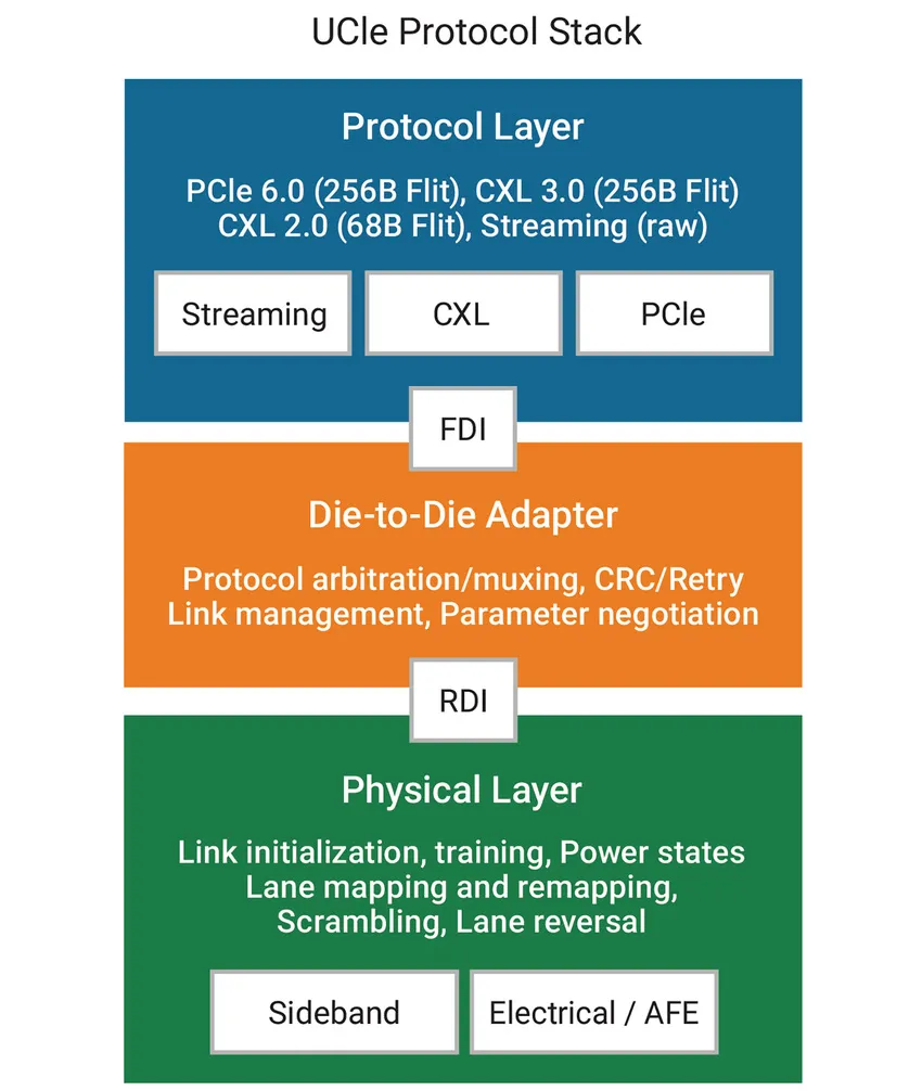
The Universal Chiplet Interconnect Express (UCIe) is the industry’s answer to this challenge. UCIe is an open specification that defines the complete die-to-die interconnect, covering the I/O physical layer, the protocol stack, and the software framework necessary for chiplets to communicate within a package. To accelerate adoption and ensure broad compatibility, the UCIe standard cleverly leverages well-established and proven industry protocols like PCI Express (PCIe) and Compute Express Link (CXL) as its primary methods of communication.
UCIe is arguably the single most important non-technical catalyst for the chiplet revolution. It aims to be the “USB for chiplets.” Just as the USB standard created a ubiquitous, interoperable ecosystem for connecting external peripherals to a computer, UCIe seeks to do the same for on-package interconnects. The standard was established by a consortium of industry leaders, including foundries, IP suppliers, fabless design houses, and cloud service providers, all of whom recognized that a closed, fragmented market would stifle innovation.
By creating a standardized “socket,” UCIe gives system designers the confidence to source chiplets from multiple vendors, knowing that they will be able to communicate seamlessly. This is the key that unlocks the open, competitive marketplace envisioned by the chiplet paradigm.
The success of UCIe will likely determine whether chiplets remain a specialized tool for industry giants or become a democratized resource that unleashes a new wave of custom silicon innovation from companies of all sizes. It is less a technology in itself and more of a foundational economic and ecosystem enabler.
about dnn tECHNOLOGY
Headquartered in Taiwan, DNN Technology is a global leader in semiconductor equipment and comprehensive solutions, specializing in used semiconductor equipment trading, laboratory and cleanroom systems construction, and technical consultancy services. With over two decades of industry experience and a team comprising more than thirty experienced technical experts, DNN Technology has successfully executed projects across over fifty countries, committed to providing customized, innovative, and efficient solutions.