Advanced Packaging Guide (Pt. 4): Solving Thermal & Material Challenges
The remarkable capabilities of advanced packaging are not magic; they are built upon a complex foundation of materials science and physics. Squeezing multiple high-power components into a microscopic space creates a tightly coupled system where performance is dictated by fundamental forces.
This article explores that underlying science. We will delve into the critical role of interposer materials—analyzing the trade-offs between silicon, organic, and glass—and explain why a holistic, multi-physics co-design approach is no longer optional but essential for managing the intricate interplay of thermal, electrical, and mechanical challenges.
4.1 The Interposer's Dilemma: A Deep Dive into Material Science
The interposer is the central nervous system of 2.5D integration technology, and its material choice dictates the fundamental trade-offs between performance, cost, and manufacturability. There is no single “best” material; instead, a diverse toolbox is emerging to address specific application needs.
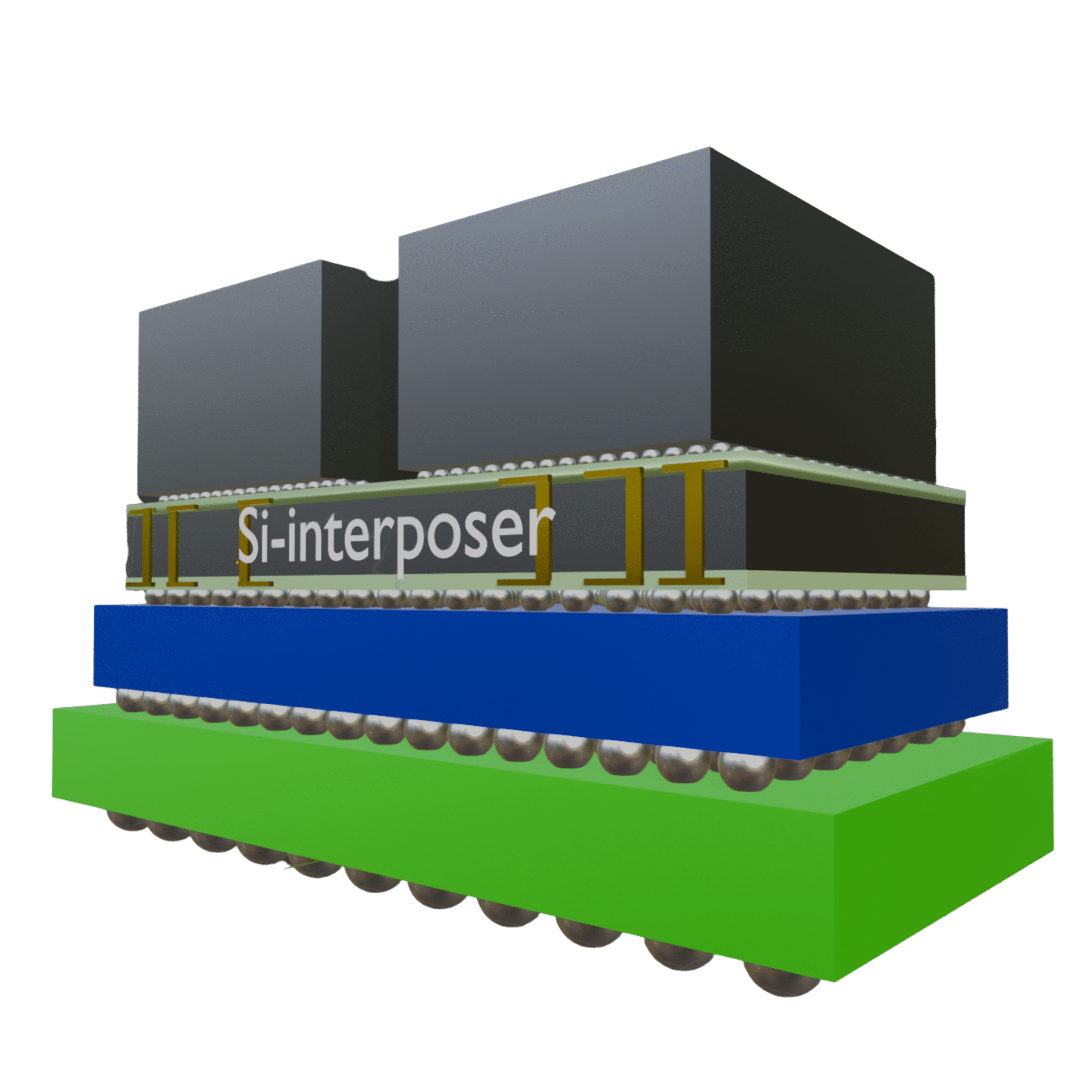
- Silicon (Si) Interposers:
As the incumbent technology for high-performance applications, silicon interposers leverage mature CMOS processes to offer unparalleled routing density (line/space L/S < 1µm). Their coefficient of thermal expansion (CTE) of approximately 3 ppm/°C perfectly matches that of silicon dies, thereby minimizing stress.
This technology is the foundation of leading solutions like TSMC’s CoWoS and is used in NVIDIA’s H100 GPU, which integrates a powerful GPU with multiple High-Bandwidth Memory (HBM) stacks on a single silicon interposer. However, its high dielectric constant (Dk) of around 11.9 can impede high-speed signal propagation, and the costs associated with large-area silicon are a significant drawback.
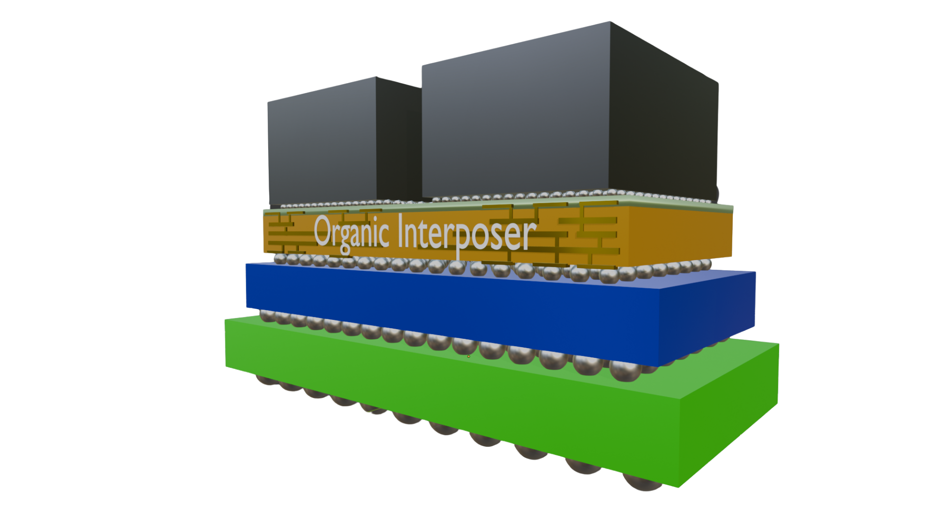
- Organic Interposers:
As a cost-effective alternative, organic interposers are gaining increasing traction. Materials such as Liquid Crystal Polymer (LCP) offer a lower dielectric constant (approx. 3.1), which is highly beneficial for signal integrity. They are more flexible and can be manufactured on larger, more economical panels. However, their routing density is lower (approx. 2-4µm L/S), and more critically, they have a severe CTE mismatch with silicon (approx. 17-50 ppm/°C), which is a primary source of package warpage and reliability issues.
- Glass Interposers:
Glass represents a highly promising future path that could offer a “best of both worlds” solution. It combines excellent dimensional stability with a low dielectric constant (approx. 4-6), and its CTE can be engineered to match silicon (approx. 3-8 ppm/°C).
The market is projected to exceed $2.4 billion by 2032. Major players including Intel, Samsung, Corning, and AMD are actively investing and filing patents to address manufacturing challenges. The primary obstacle is the immaturity of the manufacturing ecosystem, particularly the fabrication of high-aspect-ratio through-glass vias (TGVs), which is costly and suffers from low yields.
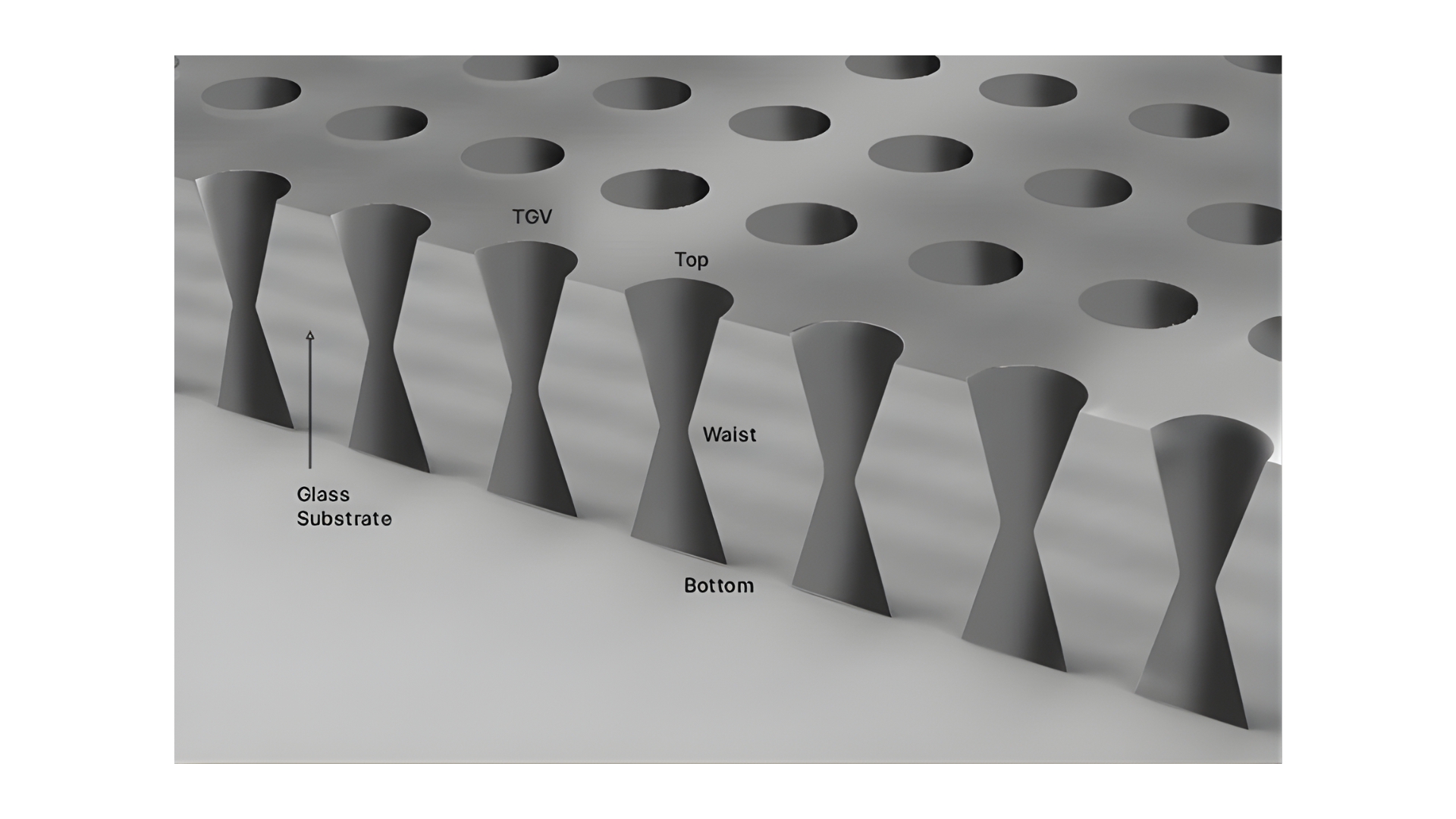
(Source: Semiconductor Engineering)
- Embedded Multi-die Interconnect Bridge (EMIB) Solution:
Technologies like Intel’s Embedded Multi-die Interconnect Bridge (EMIB) offer a clever compromise. Instead of a large, expensive silicon interposer, small, high-density silicon bridges are embedded directly into a lower-cost organic substrate precisely where high-bandwidth die-to-die communication is needed.
This approach is used in products like the Ponte Vecchio GPU, which localizes the benefits of silicon (density) while leveraging the cost and scalability advantages of an organic substrate, representing a key trend toward hybrid material solutions.
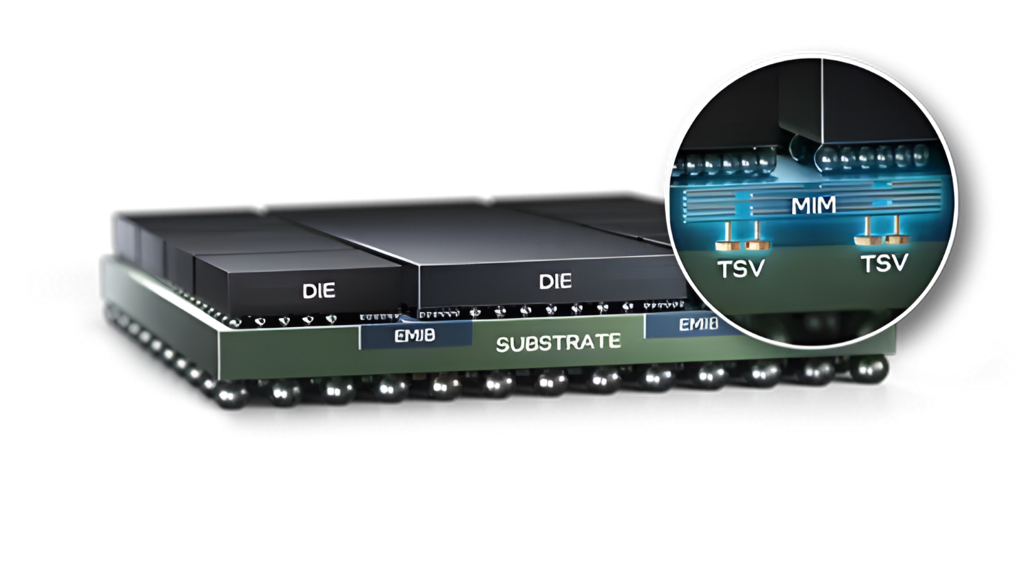
(Source: Intel)
This material selection dilemma is more than just a technical trade-off; it initiates a causal chain that extends from physics to economics. The performance demands of an AI accelerator dictate the need for extremely high interconnect density between its logic die and HBM. This density requirement pushes the design toward a silicon interposer, as organic materials cannot achieve the necessary <1µm line/space.
However, choosing a large silicon interposer and pairing it with an organic package substrate introduces a massive CTE mismatch. This mismatch creates significant thermo-mechanical stress, making package warpage and solder joint reliability primary failure modes. This reliability risk, in turn, necessitates significant investment in multi-physics simulation tools (EDA) and advanced thermal interface materials (TIMs) to mitigate stress and manage heat.
Thus, the initial performance-driven choice of a silicon interposer directly leads to significant reliability challenges, which in turn drive economic investment in mitigation technologies. This reveals how material science, physics, and economics are inextricably linked in the field of advanced packaging.
The following table provides a comparative analysis of key interposer materials, highlighting the engineering trade-offs involved.

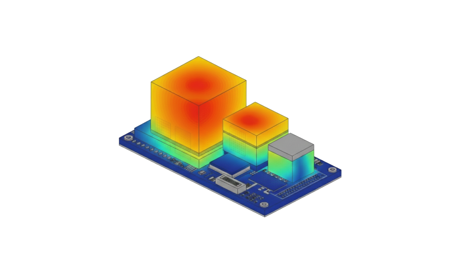
4.2 The Invisible Enemy: Taming Thermo-Mechanical Stress
The most pervasive reliability challenge in advanced packaging is thermo-mechanical stress, rooted in the fundamental mismatch in how different materials expand and contract with temperature changes. This is not a secondary issue but a primary design constraint that can lead to catastrophic failure.
- The Physics of CTE Mismatch:
During manufacturing processes (like reflow) and operation, a package undergoes significant temperature cycles. A silicon die expands at a rate of about 2.6-3 ppm/°C, while a standard organic substrate can expand at a rate as high as 17-50 ppm/°C. This vast difference forces the components to bend and warp, creating immense internal stress. This stress concentrates at the weakest links: the fragile solder joints and interconnect structures.
- The Consequences of Failure:
This stress manifests as package warpage, which can prevent proper mounting and lead to open circuits. Under repeated thermal cycling, it causes metal fatigue, resulting in cracked solder balls and delamination between layers, ultimately leading to device failure. This problem is particularly acute in large 2.5D packages due to the size of the large silicon interposer.
- The Necessity of Co-Design:
The traditional “throw-it-over-the-wall” design flow is obsolete. The tight coupling of electrical, thermal, and mechanical phenomena necessitates a multi-physics co-design approach. Electrical activity generates heat (electro-thermal), which causes materials to expand and induces stress (thermo-mechanical), and this mechanical stress, in turn, can deform the silicon lattice, altering the electrical properties of transistors and affecting timing (mechano-electrical). Modern EDA tools from companies like Ansys (now part of Synopsys) and Cadence are essential for comprehensively simulating these feedback loops, allowing architects to predict and mitigate stress before fabrication.
4.3 The Thermal Challenge: Advanced Thermal Management Solutions
As power densities skyrocket in 3D stacks and densely packed 2.5D systems, heat removal has become the ultimate physical bottleneck. Removing hundreds of watts of heat from a microscopic volume requires a paradigm shift from conventional cooling to advanced materials and disruptive technologies.
- The Role of Thermal Interface Materials (TIMs):
TIMs are crucial for bridging the microscopic air gaps between the die, lid, and heat sink. The industry categorizes them by location: TIM1 (die-to-lid), TIM1.5 (die-to-heatsink in lidless designs), and TIM2 (lid-to-heatsink). While polymer-based TIMs are common, high-performance computing (HPC) increasingly relies on superior-performing metal-based TIMs.
。 Advanced Metal TIMs:
These include solder TIMs (sTIMs), which offer the lowest thermal resistance by forming a direct metallurgical bond; liquid metals, which provide excellent wetting but require careful containment; and compressible TIMs (like Indium’s Heat-Spring®), which deliver high performance without a reflow process. The thermal conductivity of these materials (up to 86 W/mK) is an order of magnitude higher than polymer pastes, making them critical for cooling high-power AI accelerators.

(Source: DNN Technology)
- The Future: Direct Liquid and Microfluidic Cooling:
For the most extreme thermal challenges, especially in dense 3D stacks where heat is trapped between layers, air cooling is insufficient. The future lies in bringing liquid coolants directly to the silicon. Microfluidic cooling involves etching microscopic channels directly into the backside of the silicon die, allowing coolant to flow through the chip itself.
Pioneering research from companies like Microsoft has shown this approach can be up to 3 times more efficient at removing heat than advanced cold plates under specific test conditions, enabling higher performance and overclocking potential. This technology represents one of the most promising solutions for overcoming the “thermal wall” in 3D integration.
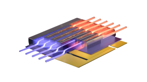
(Source: Vytautas Navikas/EPFL)
4.4 Summary
Across the packaging hierarchy, the industry is converging on hybrid solutions, demonstrating that optimization, not the purity of a single technology, is the winning strategy.
At the system level, heterogeneous integration is itself a hybrid approach, mixing chiplets from different process nodes.
At the interconnect level, technologies like Intel’s EMIB are a hybrid of high-density silicon bridges and low-cost organic substrates, taking the best of both. AMD’s MI300 architecture, with its 3D-stacked compute dies on top of a 2.5D base die with HBM, is another prime example of a hybrid 2.5D/3D architecture.
At the material level, we see the development of silicon bridges embedded in organic interposers and hybrid metal-organic heat spreaders.
This shows that the dominant philosophy is not for silicon to “win” over organic, or 2.5D to “win” over 3D, but to use the most advanced, expensive solution where it is absolutely necessary (e.g., the die-to-die interface) and leverage more cost-effective technologies for the rest of the system. This pragmatic, hybrid approach is key to balancing PPAC (Power, Performance, Area, Cost).
about dnn tECHNOLOGY
Headquartered in Taiwan, DNN Technology is a global leader in semiconductor equipment and comprehensive solutions, specializing in used semiconductor equipment trading, laboratory and cleanroom systems construction, and technical consultancy services. With over two decades of industry experience and a team comprising more than thirty experienced technical experts, DNN Technology has successfully executed projects across over fifty countries, committed to providing customized, innovative, and efficient solutions.