Advanced Packaging Guide

Advanced Packaging Guide (Pt. 5): 2026 Supply Chain, CPO & KGD Market Definition​

Advanced Packaging Guide (Pt. 5): 2026 Supply Chain, CPO & KGD Market Definition​

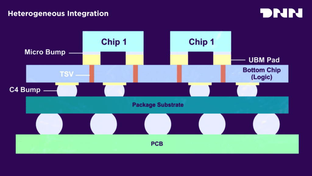
Advanced Packaging Guide (Pt. 5): 2026 Supply Chain, CPO & KGD Market Definition Recap The first four parts of this guide series have mapped out the evolutionary blueprint of the semiconductor industry in the post-Moore’s Law era. We began in Part 1 by exploring why advanced packaging has become the new frontier of innovation against […]

Advanced Packaging Guide (Pt. 5): 2026 Supply Chain, CPO & KGD Market Definition​ Read More »

Advanced Packaging : Solving Thermal & Material Challenges

Advanced Packaging Guide (Pt. 4): Solving Thermal & Material Challenges

Advanced Packaging Guide (Pt. 4): Solving Thermal & Material Challenges The remarkable capabilities of advanced packaging are not magic; they are built upon a complex foundation of materials science and physics. Squeezing multiple high-power components into a microscopic space creates a tightly coupled system where performance is dictated by fundamental forces.  This article explores that

Advanced Packaging Guide (Pt. 4): Solving Thermal & Material Challenges Read More »

Heterogeneous Integration in Advanced Packaging

Advanced Packaging Guide (Pt. 3): The Chiplet Revolution and Heterogeneous Integration​

This article focuses on that strategic shift. We will explore the move toward disaggregation by defining what “chiplets” are and why they are so compelling.

We will then explain the power of Heterogeneous Integration—the art of mixing and matching these chiplets—and detail the critical role of the Universal Chiplet Interconnect Express (UCIe) standard in creating the open, “plug-and-play” ecosystem of the future.

Advanced Packaging Guide (Pt. 3): The Chiplet Revolution and Heterogeneous Integration​ Read More »

FOWLP/2.5D INTERPOSER/3D PACKAGING

Advanced Packaging Guide (Pt. 2): 2.5D vs. 3D-IC vs. FOWLP

In the rapidly evolving world of semiconductor technology, advanced packaging is revolutionizing how we design and integrate electronic systems. Discover the transformative power of 2.5D and 3D-IC architectures, which are breaking through the limitations of traditional 2D packaging. Learn how these innovations address critical challenges like latency and power consumption, enabling high-performance applications in AI and HPC. Plus, explore the cost-effective Fan-Out Wafer-Level Packaging (FOWLP) that democratizes high-density integration for consumer electronics. Dive into our comprehensive guide to uncover the future of semiconductor packaging and its impact on the next generation of electronics!

Advanced Packaging Guide (Pt. 2): 2.5D vs. 3D-IC vs. FOWLP Read More »

A computer chip using 2.5D Advanced Packaging technology with chiplets, interposer, TSV, RDL and PCB.

Advanced Packaging Guide (Pt. 1): Why 2.5D & Chiplets Are the Mainstream Choice After Moore’s Law?

In the rapidly evolving semiconductor landscape, the traditional path of Moore’s Law is giving way to a revolutionary approach: advanced packaging. As the demand for computational power surges, innovative solutions like 2.5D and chiplet architectures are reshaping how we design and build complex electronic systems. This first article in our series delves into the critical shift from monolithic Systems-on-Chip (SoCs) to modular Systems-in-Package (SiPs), highlighting the transformative potential of advanced packaging. Discover how this paradigm shift is not just a technical evolution but a strategic necessity for the future of electronics.

Advanced Packaging Guide (Pt. 1): Why 2.5D & Chiplets Are the Mainstream Choice After Moore’s Law? Read More »

Scroll to Top